angelothewolf
Newbie
- Jun 23, 2017
- 1
- 0
- Primary Interest:
- All Treasure Hunting
Hi there!
I build this projet and im trying to get it to work,
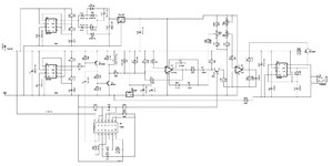
this is the schematic of the PI circuit I build,

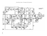
it in the net I came up with a scan of the magazine where it was first published back in 1979, so the circuit I build is a redraw of this circut with some changes or improvements? Take a look at how the voltage rails are generated in the circuit, especifically the negative regulator (78L05) for the opamps does not apears to be sharing the same ground reference as the positive regulator on the redraw of the circuit I build, so I hope some body helpme identify the problem to get this baby running...

this is a circuit description of the man who redraw the circuit>
Circuit Description
"Basically U1 is a timer integrated circuit that is wired as a pulse generator. The output on pin 3 is a negative going pulse of a width that determines the width of the transmitter pulse. This is repeated at a certain frequency that is the transmitter pulse rate. This pulse train drives T1, which inverts it so that it is then a positive pulse driving the base of T2. T2 is the transmitter output stage driving the search coil, L1, in its collector. U2 is a voltage regulator that takes the negative battery voltage and gives -5V output for the receiver amplifiers U3 and U4. R7 across the coil is a damping resistor to stop the coil ringing. The live side of the coil then goes through a 300? ohm resistor to pin 2 of U3 which is a wide band receiver amplifier. The two back to back diodes prevent the transmitter switching transients from damaging U3. After amplification the signal goes to the sampling gate T3. This acts as a switch that is closed until a short time after the transmitter pulse has ended (pulse delay) This delay is generated by the 4093 dual monostable which is triggered via C4 from the transmitter waveform. The first half on the 4093 generates the delay duration while the second half generates the time that the gate stays open. U4 is a single ended integrator which takes a running average of the samples of the amplified receiver waveform. When there is no metal near the coil the sample will be approximately zero; bring metal near to the coil and the sampled decaying waveform from the metal will cause the output of U4 to rise. This dc output goes via R17 to the transistor T4 which controls another timer IC, U5, to generate the audio pulses. The audio output is a tick that increases in frequency as metal is brought closer to the coil. The threshold tick is set by P3 that alters the bias on the other input of U4. Headphones can be connected to pins 3 and 2 of the connector on the right of the schematic. A resistor in series here might be necessary to adjust the volume. At the top left of the schematic U6, is another timer that generates a separate pulse train that is then rectified by the diodes D1-D4 to give a positive dc voltage which is then supplied to the positive 10V regulator U7 which gives the positive supply necessary for the receiver IC's. P1 is a preset resistor that sets the dc output level on pin 6 of U3 to 0 volts. It is useful to connect an oscilloscope to this point for testing to see that everything is working OK. The only thing that I can't show here are the various waveforms and their relationship with each other. These are controlled by the components around the timers and the monostables and are fixed by the values given in the schematic. So if everything is assembled right the only setup adjustment is P1." Eric Foster
I build this projet and im trying to get it to work,
this is the schematic of the PI circuit I build,

it in the net I came up with a scan of the magazine where it was first published back in 1979, so the circuit I build is a redraw of this circut with some changes or improvements? Take a look at how the voltage rails are generated in the circuit, especifically the negative regulator (78L05) for the opamps does not apears to be sharing the same ground reference as the positive regulator on the redraw of the circuit I build, so I hope some body helpme identify the problem to get this baby running...

this is a circuit description of the man who redraw the circuit>
Circuit Description
"Basically U1 is a timer integrated circuit that is wired as a pulse generator. The output on pin 3 is a negative going pulse of a width that determines the width of the transmitter pulse. This is repeated at a certain frequency that is the transmitter pulse rate. This pulse train drives T1, which inverts it so that it is then a positive pulse driving the base of T2. T2 is the transmitter output stage driving the search coil, L1, in its collector. U2 is a voltage regulator that takes the negative battery voltage and gives -5V output for the receiver amplifiers U3 and U4. R7 across the coil is a damping resistor to stop the coil ringing. The live side of the coil then goes through a 300? ohm resistor to pin 2 of U3 which is a wide band receiver amplifier. The two back to back diodes prevent the transmitter switching transients from damaging U3. After amplification the signal goes to the sampling gate T3. This acts as a switch that is closed until a short time after the transmitter pulse has ended (pulse delay) This delay is generated by the 4093 dual monostable which is triggered via C4 from the transmitter waveform. The first half on the 4093 generates the delay duration while the second half generates the time that the gate stays open. U4 is a single ended integrator which takes a running average of the samples of the amplified receiver waveform. When there is no metal near the coil the sample will be approximately zero; bring metal near to the coil and the sampled decaying waveform from the metal will cause the output of U4 to rise. This dc output goes via R17 to the transistor T4 which controls another timer IC, U5, to generate the audio pulses. The audio output is a tick that increases in frequency as metal is brought closer to the coil. The threshold tick is set by P3 that alters the bias on the other input of U4. Headphones can be connected to pins 3 and 2 of the connector on the right of the schematic. A resistor in series here might be necessary to adjust the volume. At the top left of the schematic U6, is another timer that generates a separate pulse train that is then rectified by the diodes D1-D4 to give a positive dc voltage which is then supplied to the positive 10V regulator U7 which gives the positive supply necessary for the receiver IC's. P1 is a preset resistor that sets the dc output level on pin 6 of U3 to 0 volts. It is useful to connect an oscilloscope to this point for testing to see that everything is working OK. The only thing that I can't show here are the various waveforms and their relationship with each other. These are controlled by the components around the timers and the monostables and are fixed by the values given in the schematic. So if everything is assembled right the only setup adjustment is P1." Eric Foster


